I caused many EMI problems during my career as electronics designer
Some projects where cancelled, others delayed.
I lacked practical experience, rules of thumb and EMI awareness while designing.
As junior designer, EMI seemed black magic to me at first…
- The shielding has no effect?!
- When I hold my finger here it works!
- Why does twisting the cable not help?
Failing forward increased my awareness and insight which led to:
- Less surprises
- Less fire fighting
- Realistic planning
- Increased confidence
- Less design revisions
- More fun during the design process 😎
Building your EMI competence is easy.
- Read
- Experiment
- Talk to experts
- Share your learnings
It does take a lot of time though, invest!
Or take a shortcut.
Whatever you do, prevent EMI failure by avoiding the 7 most common PCB layout mistakes listed below.
- Joost Brilman

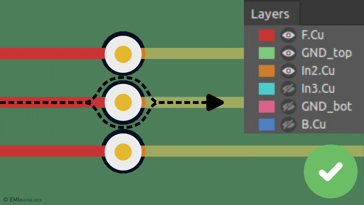
1. Unfavorable PCB layer stack-up
Emission and interference levels of a PCB are proportional to the area of the current loops.
To reduce these negative EMI effects, it is crucial to keep the current loop dimensions small.
Traces routed on a single layer create a relatively large loop area.
A reference plane at the bottom is better, but still has a relatively large loop size.
Loop dimensions are best kept small using a reference plane on a layer next to each signal trace.
Typical reference plane nets are 'GND' or '0V', the most common reference net in your design.
Keep the reference plane solid, without any traces or slits.
A reference plane near a signal trace enables high-frequency current to flow back in a small loop.
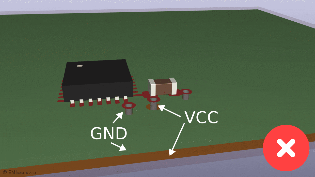
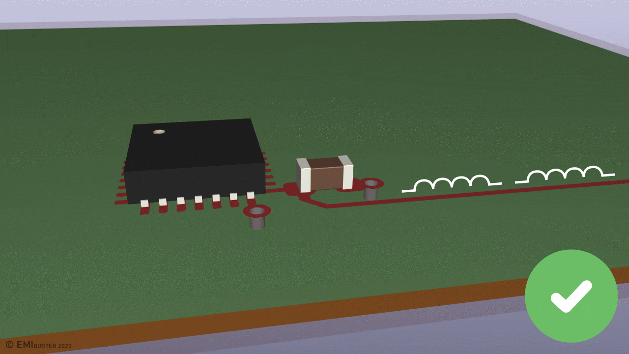
2. Bypassed Common Mode filter
Common Mode (CM) filters reduce EMI emission and reception via cables connected to the PCB.
A CM filter should act as high impedance barrier, limiting high-frequency current flow.
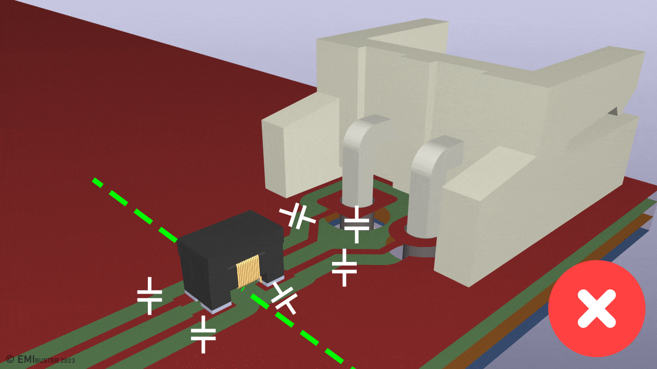
Parasitic capacitance between filter traces and other copper acts as bypass for high-frequency current.
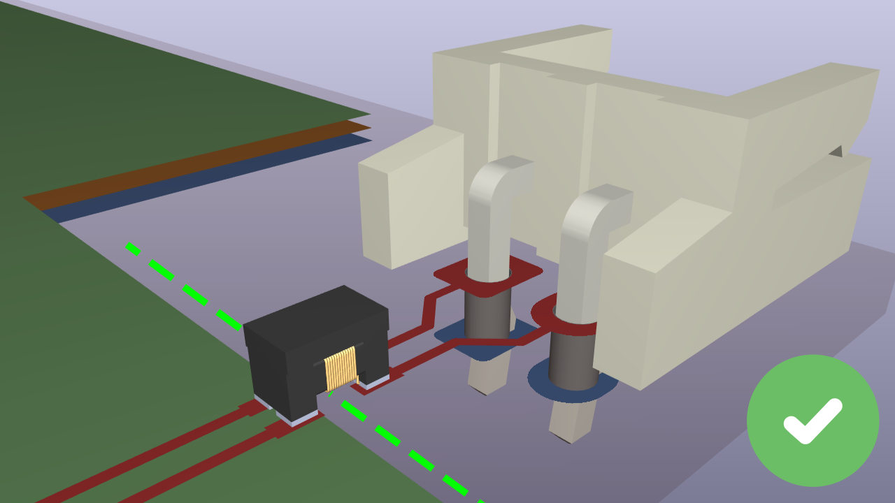
Remove unused PCB copper on every layer to prevent creating an unintentional bypass.
A low impedance bypass path diminishes the effectiveness of the filter in its intended purpose.
Place the filter at the edge of the board for a natural separation between the board and cable side.
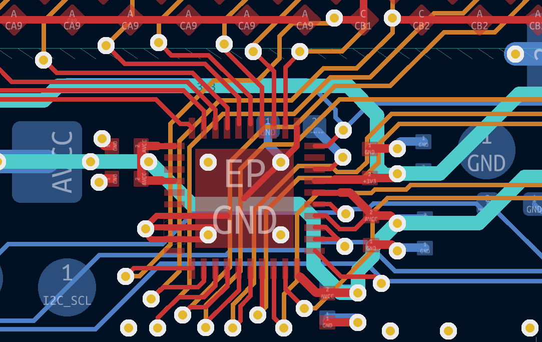
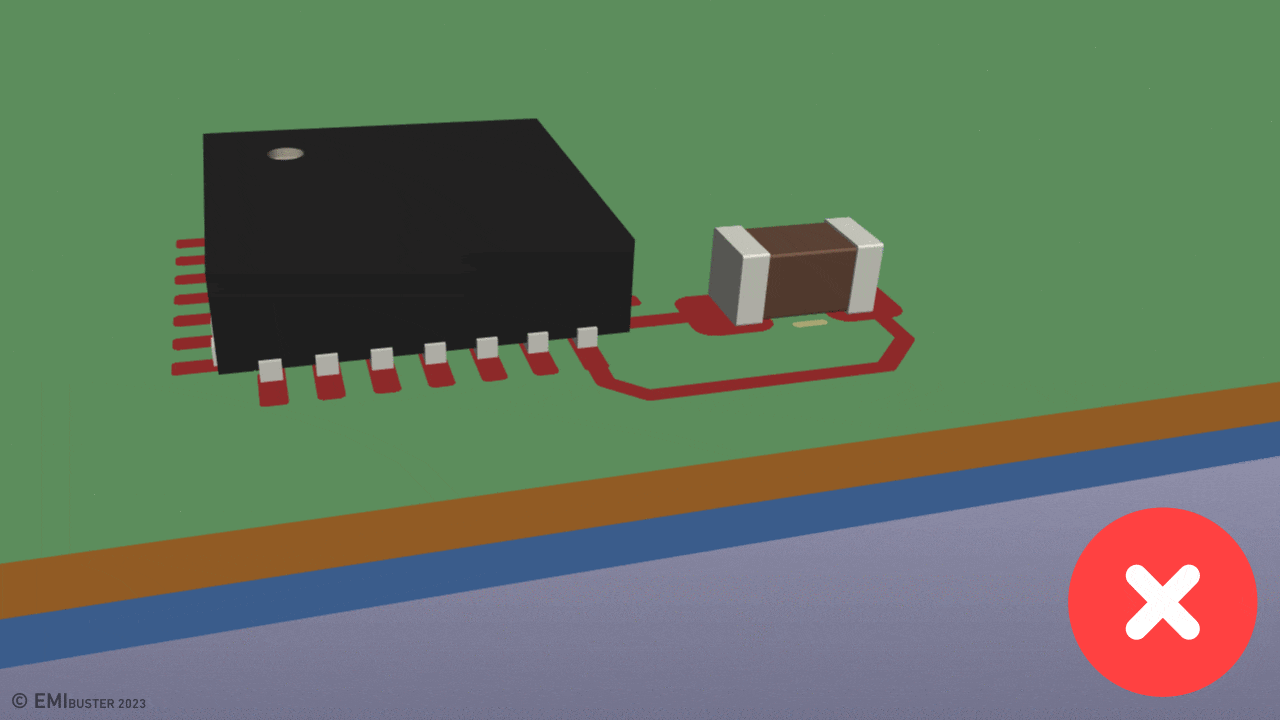
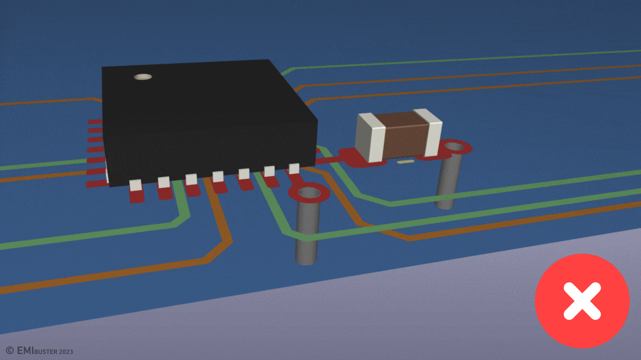
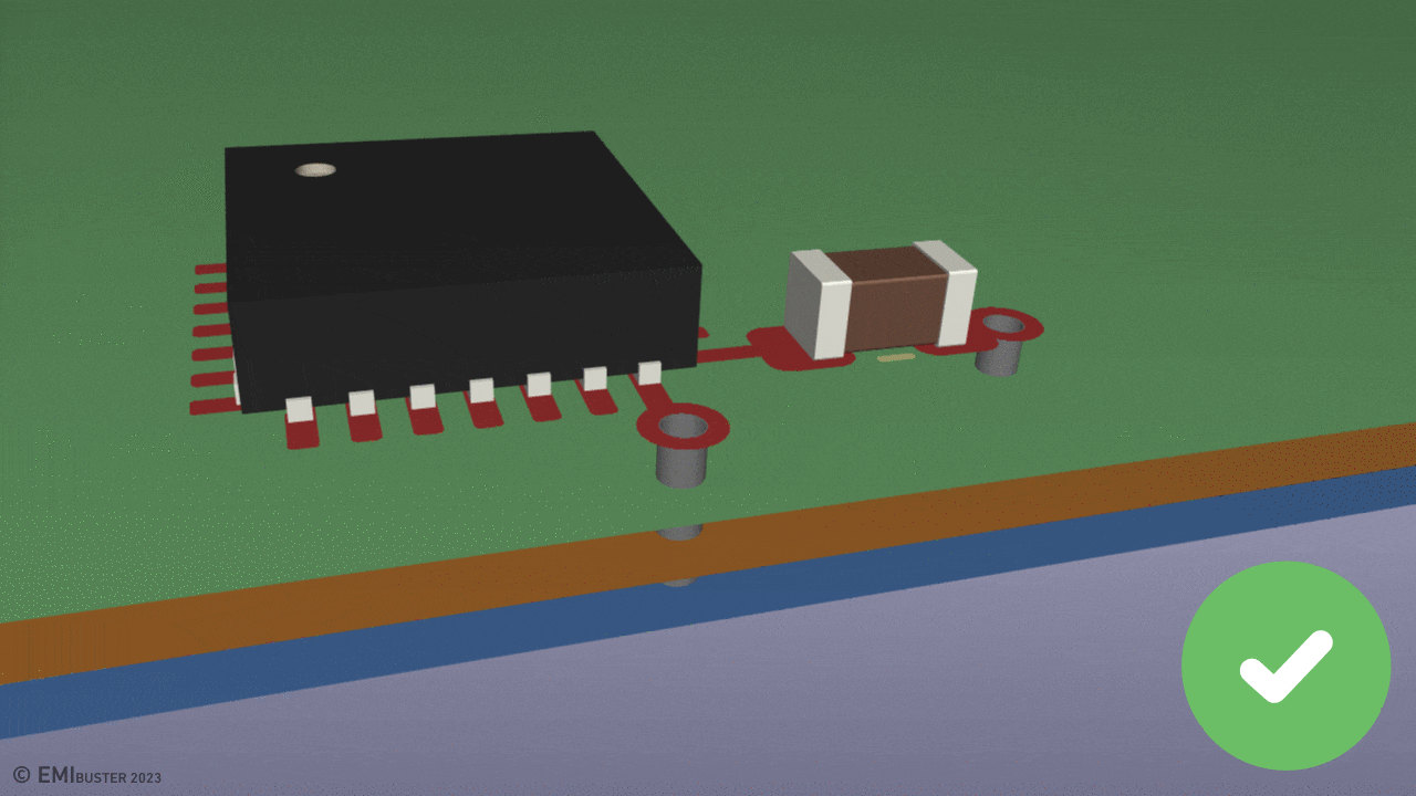
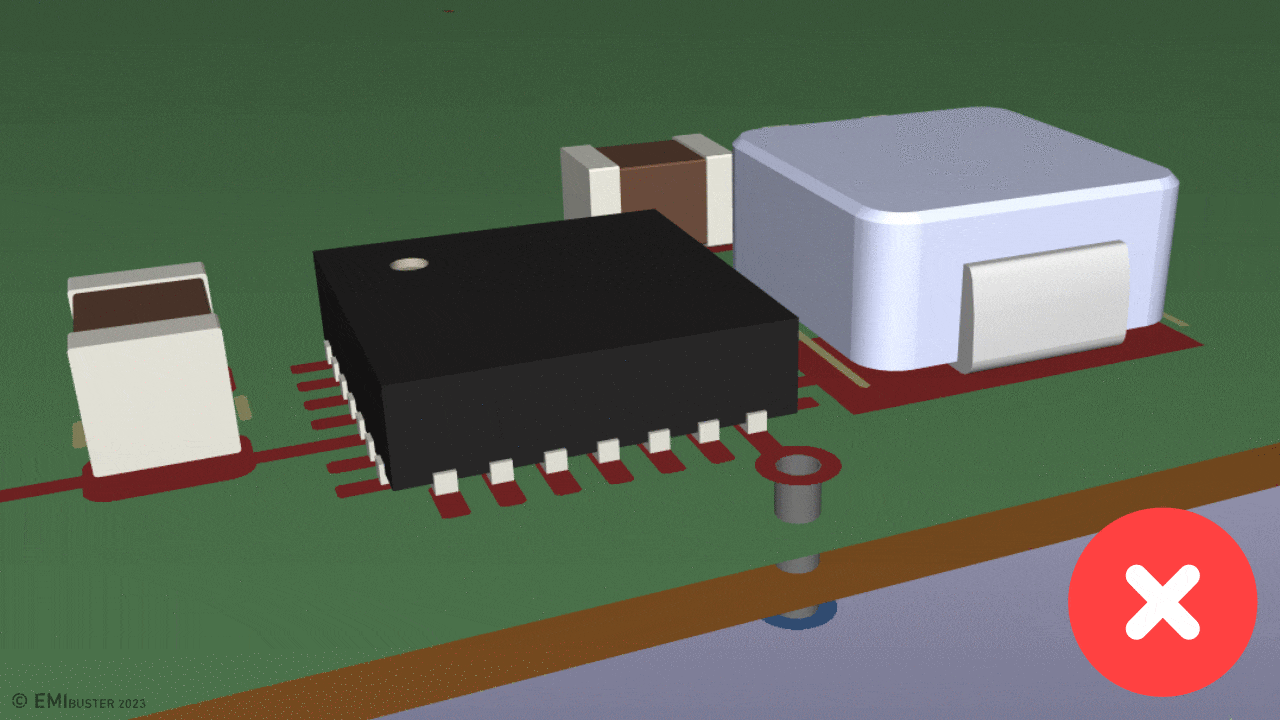
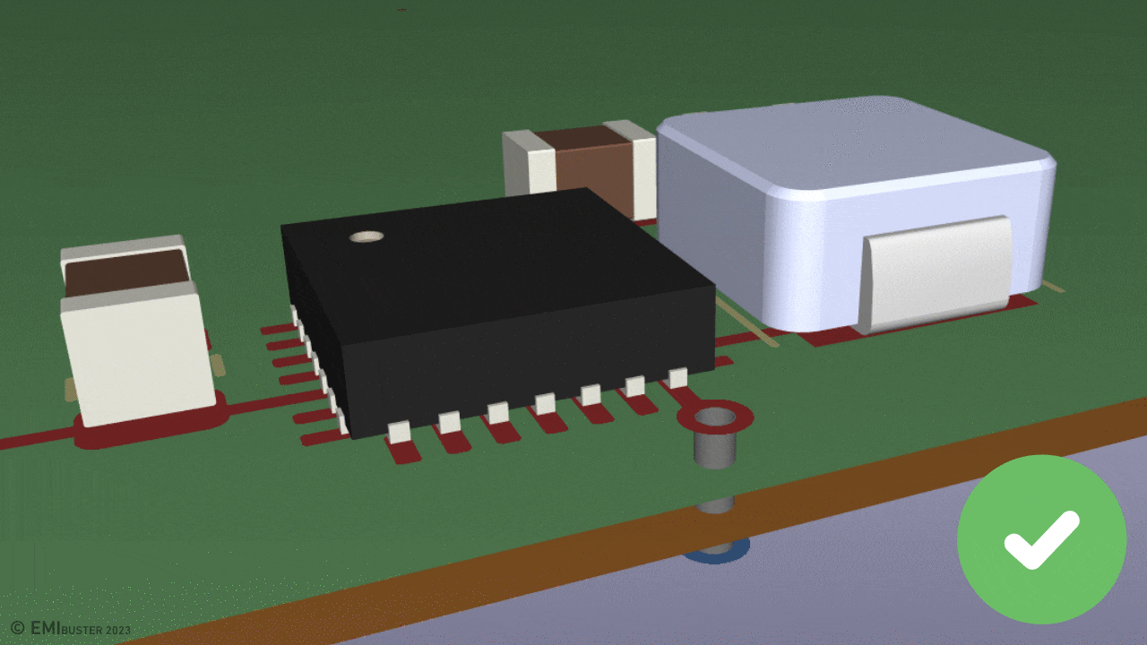
3. Placing the GND Via far from the component pin
This one is often overlooked as placing GND Via's seems easy.
Boom! Just shoot a Via in the reference plane and watch the Rats Nest disappear. Done!
Not so fast.
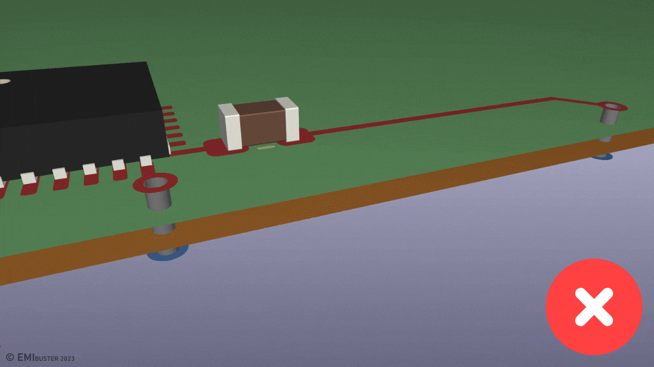
Failure to place a Via directly at the GND pads increases the current loop area.
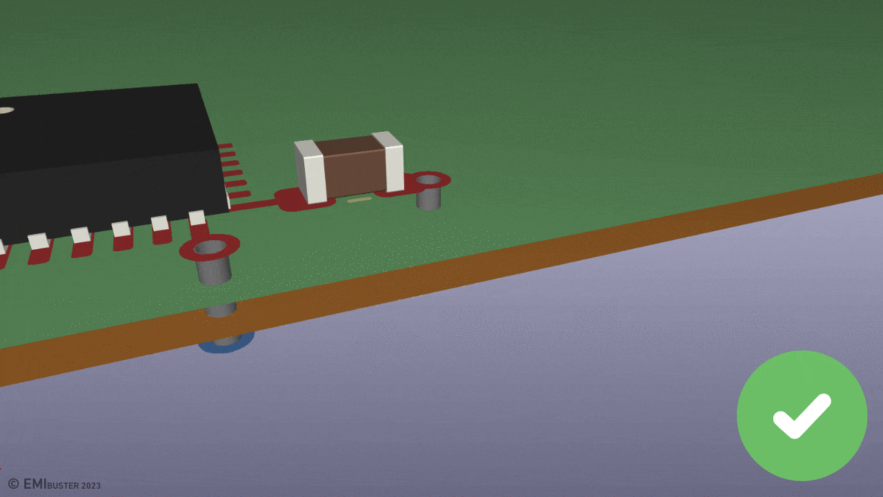
Place the Via as close as possible to the component pad to keep the loop area small.
Doing so reduces interference and emission levels.
Additionally, the decreased loop impedance will improve the effectiveness of decoupling capacitors.
4. Too large switching nodes
Switched Mode Power Supplies include a net that rapidly switches between different voltages.
This rapid voltage change (dv/dt) is a primary source of emission and interference.
Parasitic capacitance (c) between the switching net and its environment enables current to be injected into the rest of the system.
This current, determined by i=c*dv/dt, seeks a return path to the supply rails of the switching semiconductor.
Large switching copper areas increase the parasitic capacitance c, leading to larger EMI currents.
Route your switching nets copper area as small as possible to keep the capacitive coupling low.
5. Top to Bottom transition
Fast switching (digital) signals hate Vias!
Try to avoid them.
What if a layer transition is unavoidable?
Remember that a reference plane should be present at the layer adjacent to each signal trace.
If a signal switches board side, it's reference plane switches board side as well.
Board side transition with a single Via forces a large return current loop through a remote Via.
Connect the reference planes close to the signal-Via to keep the current loop area small.
The return current will always find a path back to its source. Make sure a small loop path is available to reduce emission and interference levels.
6. Use of power planes
Power planes are efficient in the layout process. Just shoot some Vias. Boom! Connected!
Let's look at it from an EMC perspective.
A power plane next to a reference plane acts like a capacitor with low parasitic inductance.
This is great for decoupling high-frequency currents.
Not so great for keeping the high-frequency current loops small.
A plane capacitor disperses the high-frequency decoupling currents throughout the entire board.
Use traces for DC supply distribution and place decoupling caps near the switching devices.
Minimizing high-frequency current loop area is key to achieve desirable EMC performance.
FPGA like IC's demand high supply current peaks. For those systems a local power plane is often required for proper decoupling. Local, so don't cover your whole board.
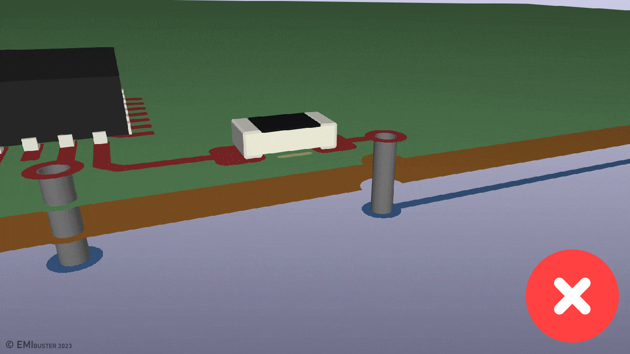
7. Reference plane slit due to improper Via placement
Vias placed too close to each other create a significant slit in the reference planes.
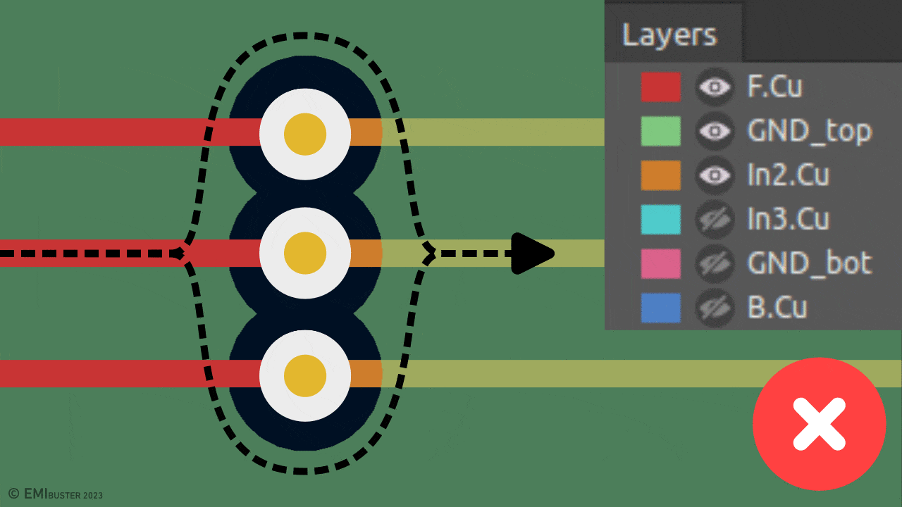
Return current has to take a detour loop.
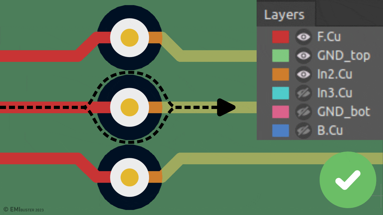
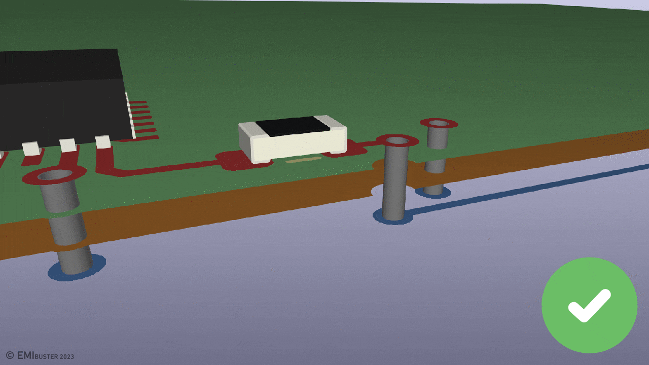
Increased Via spacing enables return current to flow between them.
Reduced clearance reconnects the plane inbetween the Vias.
A reference plane slit disrupts the flow of return currents, forcing them to travel in a loop around the slit boundary. ❌
Large current loops lead to increased emission and interference levels on the PCB.
Ensure that the return plane is connected between the Vias. ✔️
Keeping the return plane as solid as possible keeps the loop areas small and the emissions low.